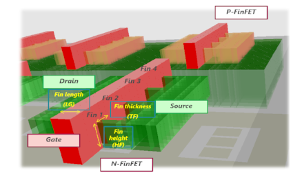
14-NM FinFET in Microwind

Microwind framework has been now configured to simulate FinFET transistors ; which are tuned to technology parameters close to 14-nm from Intel.

FinFET advantages

Instead of a continuous channel,
the FinFET uses fins, allowing transistor be low power,
faster, compact and continue scaling.
FinFET provides the same Ion current at a smaller size.
FinFET provides lower leakage current Ioff at the same Ion.
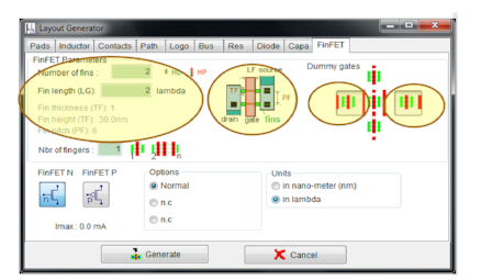
Microwind will now allow student to explore future
technology which is different from 45 years old planar style.
Learn about process variation and manufacturability issue
with/without dummy gates.
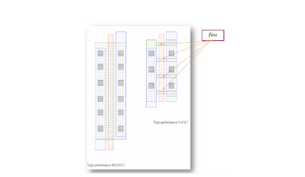
Planar MOS were almost about to break Moore’s law,
know how FinFET kept it intact.

FinFET Technology

FinFET, also known as Fin Field Effect Transistor, is a type of non-planar or "3D" transistor used in the design of modern processors. FinFET designs also use a conducting channel that rises above the level of the insulator, creating a thin silicon structure, shaped like a fin, which is called a gate electrode. This fin-shaped electrode allows multiple gates to operate on a single transistor. This type of multi-gate process extends Moore's law, allowing semiconductor manufacturers to create CPUs and memory modules that are smaller, perform faster, and consume less energy.

FinFET generator in Microwind

In Microwind 3.8 you can generate FiNFET transistors or compiler using Verilog file too. Below are the outline of generated transistor.
Fin Length, equal to gate length, (LG) is 2 lambda
(16 nm) by default
Fin thickness (TF) is set to 1 lambda (8 nm)
Fin pitch (PF) is set to 6 lambda (48nm)
FinFET comme with dummy gates for manufacturability
HD: High density drawing style : 2 fins
HP : High performance drawing style : 4 fins

Ready to learn about CMOS