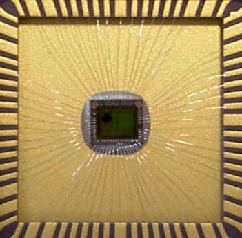
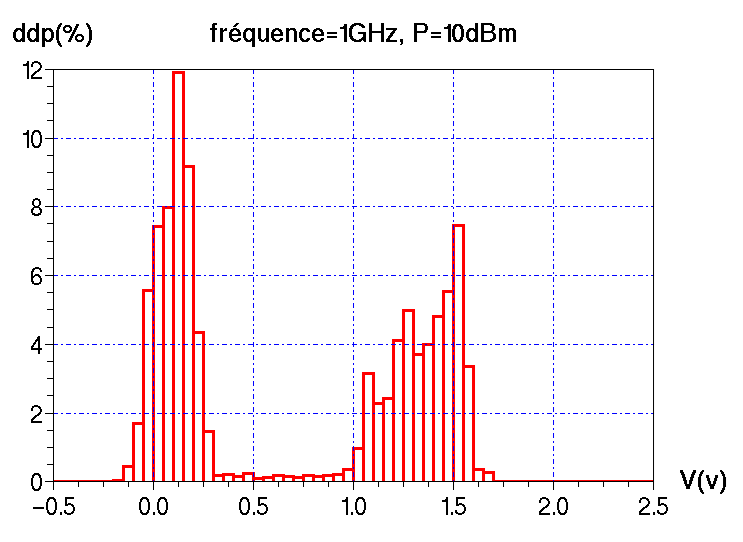
The Alfa2 test-chip has been designed, fabricated in a CMOS 0.18µm technology and successfully tested. The chip included innovative on-chip random sampling for measuring susceptibility to mobile-phone interference. Critical basic cells have been designed and simulated using Microwind 2.7.
Designers
Designers involved in the project are Sonia Bendhia, senior lecturer INSA Toulouse, Enrique Lamoureux, PhD student at INSA Toulouse, and Bertrand Vrignon PhD student ST-Microelectronics
Frame
The IC Alfa2 was financed by the European ALFA program which supports joint co-operation projects between European and Latin American higher education institutions, to strengthen the links between higher education institutions of both continents. The IC included 10 different test patterns (MOS devices, logic cores, analog circuits, OpAmps, advanced on-chip measurement systems, etc..)
Role of Microwind
Microwind was given to all partners who designed MOS, interconnects and Electromagnetic-compatibility experiments separately. Once tested, the layout was converted into CIF format for full verification and final assembly of the test-chip under third party Design Framework. The IC was sent to ST-Microelectronics to the CMP service available at TIMA, France.<
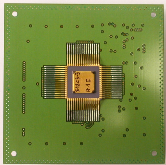
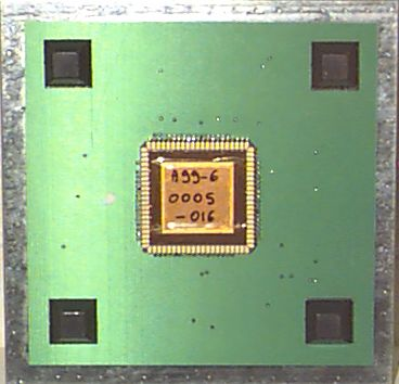
The Biomi2 test-chip has been designed, fabricated in a CMOS 0.8 µm technology and successfully tested. The chip included a programmable pulse generator. The logic design has been fully conducted using Dsch. The layout has been compiled in Verilog by Microwind converted into CIF for final verification using professional tools.
Designers
Designers involved in the project are Chen Xi, PhD student at INSA Toulouse, Etienne SICARD, professor at INSA Toulouse, and Jean-Louis Noullet, and a senior lecturer.
Frame
The IC Biom2 was financed by the regional Council under a research program on programmable implants for neuro-stimulation, in cooperation with the company Newmedic, France. The IC Biomi2 included different prototype structures to validate the design flow and the logic chip architecture.
Role of Dsch and Microwind
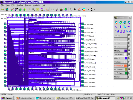
Dsch was used for the complete logic design and simulation. Dsch performed for the simulation of more than 1000 symbols. The user’s interface was constantly improved to handle such a complex design. Microwind was also significantly improved to handle the automatic conversion from Verilog to layout. Numerous iterations were necessary to complete working silicon. The layout was exported in CIF format to third party Design Framework for full design rule checking. The IC was fabricated through the TIMA/CMP facility by Atmel-ES2, in CMOS 0.8µm double-metal technology.