NANO LAMBDA
Precision CMOS layout editor, with nanotechnology support.
Description
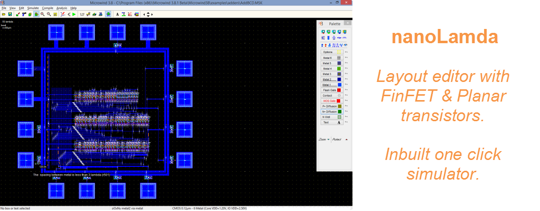
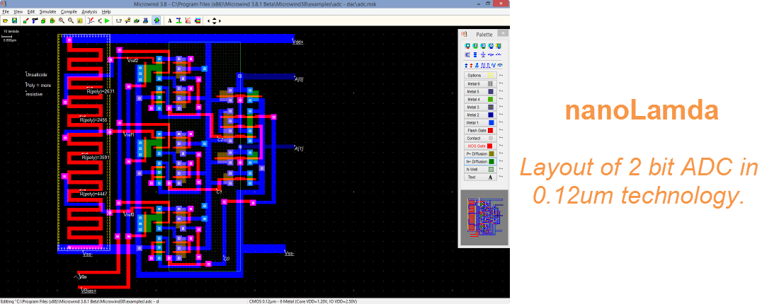
MICROWIND possess a precision CMOS layout editor, which supports technologies right from 1.2µm till 3 nm nsFET Technology with unsurpassed illustration capabilities. With its enhanced editing commands and layout control your development times would be shorter than you ever imagined. The layout editor support various technology transistors like MOSFET, FinFET, nsFET.
Highlights
 Supports MOSFET and FinFET technology till nanometer range.
- Introduction of Nanosheet Field Effect Transistor (NSFET) with 3nm technology.
- Improved layout structure for NSFET and FinFET, design rules and visualization of transistors
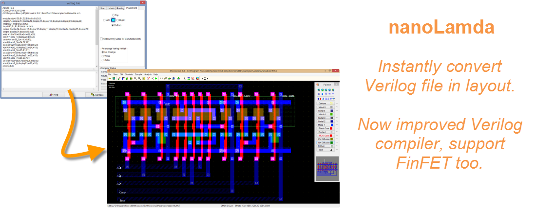
- Convert layout into schematic.
- Sub-micron, deep-submicron, ultra deep-submicron, nanoscale technology support.
- Design-error-free cell library (Contacts, vias, MOS devices, etc.).
- Advanced macro generator (Capacitor, MOS transistor, matrix, ROM, pads, inductors, path, etc.)
- Virtual components library (R,L,C, etc) for faster simulation response.
- Incredible translator from logic expression into compact design-error free layout.
- New DRC lister, now visualize DRC errors and navigate to error location with ease.
- Powerful automatic compiler from Verilog structure circuit into layout.
- Improved Verilog netlist restructuring with options of gate and wire optimization.
- Built-in extractor which generates a SPICE netlist from layout.
- Integrated third party SPICE simulation control inbuilt now.
- Extraction of all MOS width and length.
- Parasitic capacitance, inductance, crosstalk and resistance extracted for all electrical nodes.
- Modular design support with insert mask layout facility.
- Import/Export CIF layout from 3rd party layout tools.
- Supports up to 100,000 elementary boxes.
- Lock & unlock layers to protect some part of the design from any changes.
- Hide layers from palette, so that user can dig inside the layout patterns.
- Support upto 8 metal layers for DSM technologies.
- Global delay evaluation of circuit with facility to dump RC values.
- Global cross talk analyzer.
- Inversion of diffusions boxes.
- Easy label listing.
- Enhanced mathematical signal description for advance users.
- Zoom in navigator.
- Enhanced memory utilization for faster simulation.
- Silicon atom viewer with 3D support allows students to understand Si atom structure.